Broadcom Delivers Industry’s First 3.5D F2F Technology for AI XPUs
05 Dezembro 2024 - 11:00AM

Broadcom Inc. (NASDAQ: AVGO) today announced the availability of
its 3.5D eXtreme Dimension System in Package (XDSiP™) platform
technology, enabling consumer AI customers to develop
next-generation custom accelerators (XPUs). The 3.5D XDSiP
integrates more than 6000 mm2 of silicon and up to 12 high
bandwidth memory (HBM) stacks in one packaged device to enable
high-efficiency, low-power computing for AI at scale. Broadcom has
achieved a significant milestone by developing and launching the
industry's first Face-to-Face (F2F) 3.5D XPU.
The immense computational power required for
training generative AI models relies on massive clusters of 100,000
growing to 1 million XPUs. These XPUs demand increasingly
sophisticated integration of compute, memory, and I/O capabilities
to achieve the necessary performance while minimizing power
consumption and cost. Traditional methods like Moore's Law and
process scaling are struggling to keep up with these demands.
Therefore, advanced system-in-package (SiP) integration is becoming
crucial for next-generation XPUs. Over the past decade, 2.5D
integration, which involves integrating multiple chiplets up to
2500 mm² of silicon and HBM modules up to 8 HBMs on an interposer,
has proven valuable for XPU development. However, as new and
increasingly complex LLMs are introduced, their training
necessitates 3D silicon stacking for better size, power, and cost.
Consequently, 3.5D integration, which combines 3D silicon stacking
with 2.5D packaging, is poised to become the technology of choice
for next-generation XPUs in the coming decade.
Broadcom’s 3.5D XDSiP platform achieves
significant improvements in interconnect density and power
efficiency compared to the Face-to-Back (F2B) approach. This
innovative F2F stacking directly connects the top metal layers of
the top and bottom dies, which provides a dense and reliable
connection with minimal electrical interference and exceptional
mechanical strength. Broadcom’s 3.5D platform includes IP and
proprietary design flow for efficient correct-by-construction of 3D
die stacking for power, clock and signal interconnects.
Key Benefits of Broadcom's 3.5D XDSiP
- Enhanced Interconnect
Density: Achieves a 7x increase in signal density between
stacked dies compared to F2B technology.
- Superior Power Efficiency: Delivers a 10x
reduction in power consumption in die-to-die interfaces by
utilizing 3D HCB instead of planar die-to-die PHYs.
- Reduced Latency: Minimizes latency between
compute, memory, and I/O components within the 3D stack.
- Compact Form
Factor: Enables smaller interposer and package sizes,
resulting in cost savings and improved package warpage.
Broadcom’s lead F2F 3.5D XPU integrates four
compute dies, one I/O die, and six HBM modules, leveraging TSMC's
cutting-edge process nodes and 2.5D CoWoS® packaging technologies.
Broadcom's proprietary design flow and automation methodology,
built upon industry-standard tools, has ensured first-pass success
despite the chip’s immense complexity. The 3.5D XDSiP has
demonstrated complete functionality and exceptional performance
across critical IP blocks, including high-speed SerDes, HBM memory
interfaces, and die-to-die interconnects. This accomplishment
underscores Broadcom's expertise in designing and testing complex
3.5D integrated circuits.
“Advanced packaging is critical for next
generation XPU clusters as we hit the limits of Moore’s Law. In
close collaboration with our customers, we have created a 3.5D
XDSiP platform on top of the technology and tools from TSMC and EDA
partners,” said Frank Ostojic, Senior Vice President and General
Manager, ASIC Products Division, Broadcom. “By stacking chip
components vertically, Broadcom's 3.5D platform enables chip
designers to pair the right fabrication processes for each
component while shrinking the interposer and package size, leading
to significant improvements in performance, efficiency, and
cost.”
“TSMC and Broadcom have collaborated closely
over the past several years to bring together TSMC’s most advanced
logic processes and 3D chip stacking technologies with Broadcom’s
design expertise,” said Dr. Kevin Zhang, Senior Vice President of
Business Development & Global Sales and Deputy Co-COO, Taiwan
Semiconductor Manufacturing Company. “We look forward to
productizing this platform to unleash AI innovations and enable
future growth.”
“With over a decade-long partnership, Fujitsu
and Broadcom have successfully brought multiple generations of
high-performance computing ASICs to the market,” said Naoki Shinjo,
SVP and Head of Advanced Technology Development, Fujitsu.
“Broadcom’s latest 3.5D platform enables Fujitsu’s next-generation
2-nanometer Arm-based processor, FUJITSU-MONAKA, to achieve high
performance, low power consumption and lower cost.”
With more than five 3.5D products in
development, a majority of Broadcom’s consumer AI customers have
adopted the 3.5D XDSiP platform technology with production
shipments starting February 2026. For more information on
Broadcom’s 3.5D custom compute platform, please click here.
About BroadcomBroadcom Inc. (NASDAQ: AVGO) is a
global technology leader that designs, develops, and supplies a
broad range of semiconductor, enterprise software and security
solutions. Broadcom's category-leading product portfolio serves
critical markets including cloud, data center, networking,
broadband, wireless, storage, industrial, and enterprise software.
Our solutions include service provider and enterprise networking
and storage, mobile device and broadband connectivity, mainframe,
cybersecurity, and private and hybrid cloud infrastructure.
Broadcom is a Delaware corporation headquartered in Palo Alto, CA.
For more information, go to www.broadcom.com.
Broadcom, the pulse logo, and Connecting everything are among
the trademarks of Broadcom. The term "Broadcom" refers to Broadcom
Inc., and/or its subsidiaries. Other trademarks are the property of
their respective owners.
Press Contact: Khanh LamBroadcom Global
Communicationspress.relations@broadcom.comTelephone: +1 408 433
8649
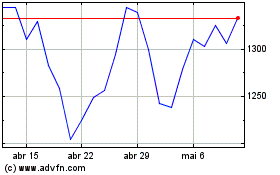
Broadcom (NASDAQ:AVGO)
Gráfico Histórico do Ativo
De Dez 2024 até Jan 2025

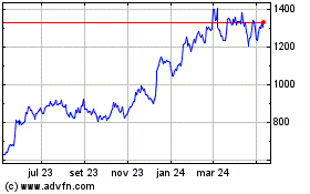
Broadcom (NASDAQ:AVGO)
Gráfico Histórico do Ativo
De Jan 2024 até Jan 2025
